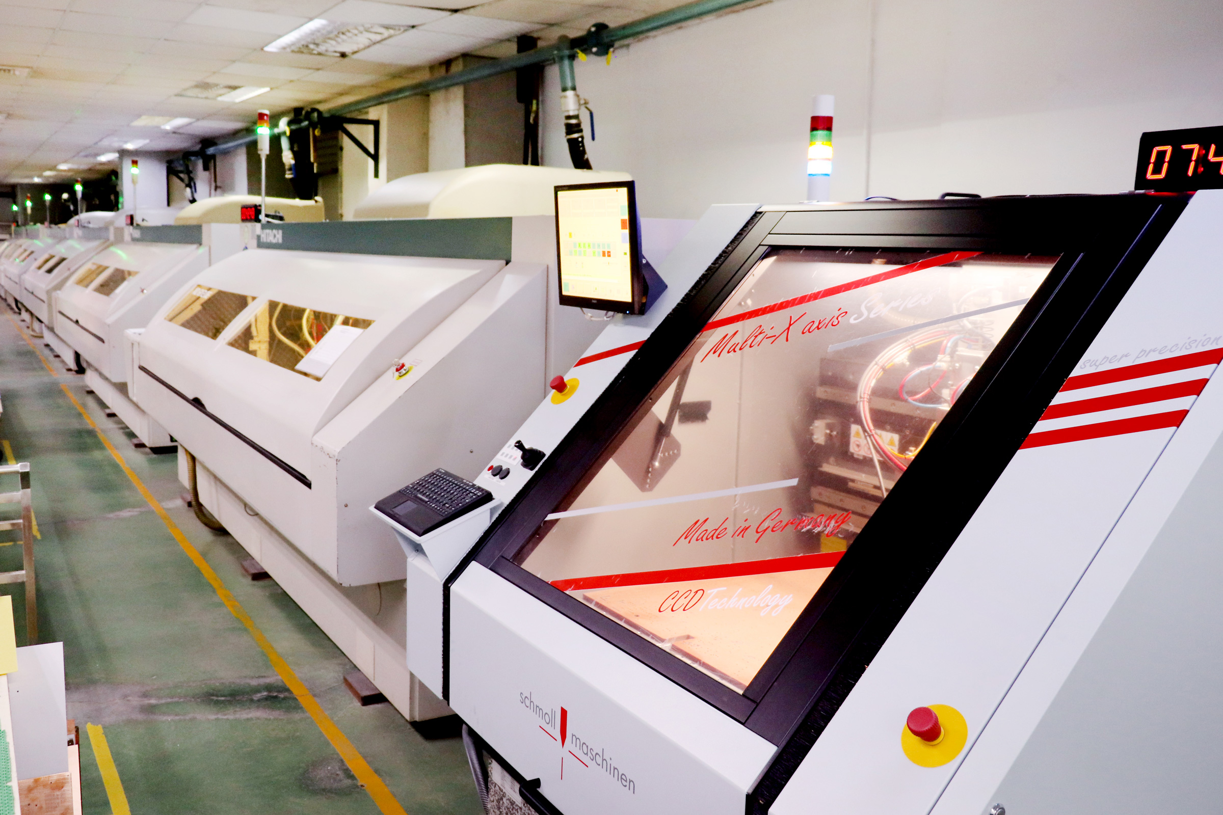
HDI circuit boards - high-density wiring and smallest vias
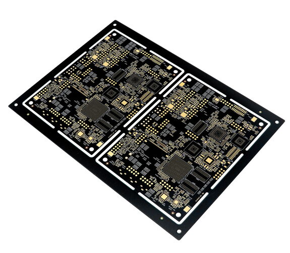
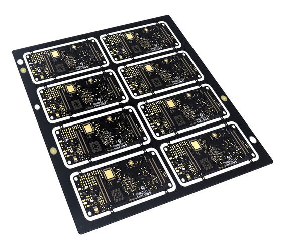
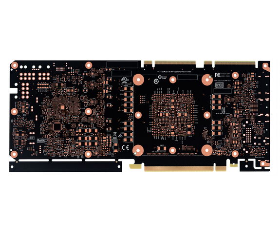
With high-density interconnection (HDI) technology, greater packing densities of electronic components can be realized. HDI PCBs offer finer line structures and require vias to implement the high-density wiring.
For the assembly and connection technology (AVT), microvias, a special form of blind vias, are used on HDI PCBs. Microvias are mechanically or more and more frequently laser drilled connections between two, maximum three layers of the PCB. With via in pad technology, microvias can be placed directly in the solder pads. The connection of the inner layers of the multilayer can be implemented in two variants. Staggered, i.e. in steps, or stacked, i.e. the microvias are stacked on top of each other. However, this requires that at least the inner microvias are designed as copperfilled vias.
Via in pad technology with microvias makes the outer layer available for unbundling, and with trace widths and spacings ≤ 0.12 mm, BGA footprints can be optimally unbundled. The significant reduction of vias PTHs frees up areas and, with optimal use, unbundling layers can be reduced.
Another option for HDI boards are internal vias, so-called burried vias. These can be designed as resin-filled or plugged variants. Plugged vias have the option of being closed by means of copper plating (IPC type VI/VII).
Advantages
- Higher wiring or connection density
- Higher packing density through technology reduces the space requirement
- finer wire structures and smaller vias through microvias
- reduces board size and number of layers if required
- alternatively creates more space for components
- unbundling possibility of smallest BGA pitch
- High conductivity due to the commonly used copper filling of the vias
- Improved thermal properties due to heat dissipation via the microvias
- High reliability during thermal cycles due to the small dimension of microvias
- Denser conductor routing
- Reduction of parasitic inductances and capacitances
- Improved signal integrity
- Structure with any number of layers with microvias creates extensive possibilities for layout design (stacked vias)
- Particularly suitable for miniaturized electronics
Definition of HDI circuit boards
- Blind via: A contact from an outer layer connected to one or more inner layers.
- Buried Via: A via located in the inner layers, connecting at least two inner layers and not visible on the outer layers.
- Microvia: Blind via with a typical hole diameter ≤ 0.15mm and holes (usually drilled by laser) with an aspect ratio of just under 1:1.
- Via Plugging:
a) Filled vias with resin or solder resist, IPC Type V, VIb
b) Filled vias with resin and copper plated over, IPC Type VII e.g., VIPPO- Via, Via in Pad plated over - Stacked Via: A special method of connecting with microvias, each placed on top of the underlying copper-filled microvia.
Application examples:
- Control unit, automotive, satellite, microsystem, industrial technology
- Communication electronics
- Camera and video surveillance for "autonomous driving”
Technology spectrum
- Use of HDI microvias in multilayers (4-48 layers)
- 1+, 2+, 3+ configurations with staggered and stacked microvias
- Microvia hole diameter from 0.05 mm to 0.15 mm
- Copper-filled microvias for stacked structures in any-layers
